PCB Assembly (PCBA) Design Guide
PCB Assembly
A printed circuit board or PCB is a central piece of any electronic device. It has two primary
functions:
- House the electronic components
- Connect components for operation
The board itself is made of a non-conducting substrate, such as fiberglass, that is coated with copper on one or both sides. The copper conducts electricity and is etched away from the board, leaving the appropriate components to be connected to each other through the circuit.
What is a PCB?
A light pipe is placed very close to an LED light source on one end of a PCB board. Its optical-grade materials help carry the rays of light to the desired destination, typically at the user interface of a device.
Light pipes transmit roughly 80 to 90 percent of the light from the LED source, depending on design and spacing. The closer the light pipes are to the LED(s), the more efficiently they can transfer light.
Of course, the light pipe(s) used will need to be rated for the same amount of heat that is produced by the LED or light source, so that must be a design consideration as well that can dictate the minimum allowable distance between the light pipe and the light source.
PCB vs. PCA vs. PCBA. What Do You Call a PCB with all the Components?
Depending on the equipment and the design of the user interface of a device, a product can require more than one and up to many indicators. For designs that require multiple indicators, light pipes are an ideal solution due to their low cost, excellent visual communication, and design flexibility.
Light pipes offer many advantages in efficiently transporting light in a defined area. But they can also transport the energy of electromagnetic waves, such as UV, infrared (IR), visual light, laser, and other types.
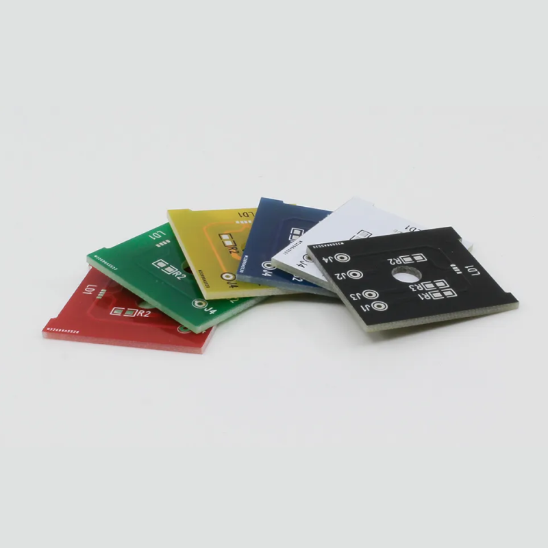
There are many acronyms that industry pros use when it comes to printed circuit boards. The most common question is, what’s the difference between a PCB and PCBA?
Here’s a breakdown of what they mean:
- PCB - printed circuit board. Technically speaking, the term PCB refers to the etched wiring board itself without any of the components installed yet. In 1999, this term was mandated by the IPC Technical Activities Executive Committee as the go-to term for new document development, as the printed circuitry design often has an impact on device function.
- PCBA - printed circuit board assembly. It’s the printed circuit board with all of the electronic components installed.
PCB is the most popular term for the whole, assembled (programmed and tested) component. So be sure to clarify which type of PCB you need when communicating with manufacturers and outside vendors — the basic board or the fully connected printed board assembly (PCBA).
How Do Printed Circuit Board Assemblies Work?

What Are Some of the Components of a PCB?
Each of the PCB hardware components has a vital role to play in powering the electronic device. Examples of PCB components include:
- Diode - an electronic component made of semiconductor material that conducts current in one direction, while blocking it in the opposite direction.
- LED - a light-emitting diode is a diode that gives off visible light when forward biased.
- Resistor - a passive element designed to resist the flow of electric current in a circuit.
- Capacitor - a passive element designed to store energy in its electric field and the voltage on a capacitor cannot change abruptly.
- Inductor - a passive element designed to store energy in its magnetic field and exhibits opposition to the change of current flowing through it.
- Switches - allow or prevent current from moving, depending on whether they are open or closed switches.
All of these PCB components are housed within the board, which is composed of multiple layers, including a substrate, copper, solder mask, and silkscreen.
What is a PCB Made Of?
The board itself is made of four key components:
- Substrate - the foundation of the PCB, a substrate is usually made of fiberglass or some other non-conductive material. Substrates can be single or multiple layers.
- Copper - used to transmit electric current, the copper within a PCB takes the place of wires.
- Solder mask - a layer that protects the electronic traces underneath from unfavorable conditions.
- Silkscreen - a layer of ink traces that are used to label electronic components, warnings and other features unique to that device’s connectivity.
Before moving into the production of final PCB production, a prototype must be validated to ensure all components are connected and work properly to power the device.
PCBs Vary in the Number of Layers Needed
How many layers do you need to get the job done?
- Single-layer PCB - a board made of a single base material or substrate layer. Typically, one side of the base material is coated with a thin metal layer on one side of the substrate. Single-layer PCBs are ideal for rapid production due to their simplicity in design and ease of automation.
- Double-layer PCB - a board that contains soldered electrical connections on both sides. This is achieved when copper or another conductive material is applied to both sides of the board. Double-sided PCBs can utilize a through-hole or surface mount (SMT) design for added flexibility.
- Multi-layer PCB - used in more complex designs, multi-layer boards include more than two layers. Multi-layer PCBs provide added benefits of a smaller footprint and fewer wiring harnesses, which reduces the overall weight. These PCBs are ideal for aerospace, handheld devices, cell and signal transmission, and many other applications.
PCBs deliver many benefits for engineers, OEMs, and designers of electronic devices, including:
- Minimal space requirements - because all electronic connections occur on the board, there’s no need for multiple wires to carry the current and take up valuable real estate on the device.
- Simplified installation and troubleshooting - all components are housed on the PCB and clearly labeled, allowing for easy access during assembly and maintenance.
- Streamlined assembly - PCBs allow for quick assembly compared to other means, such as wired connections.
- Secure placement and connectivity - with a PCB, all electronic components are soldered to the board, ensuring they will stay in place.
- Manufacturing efficiency - PCBs are more cost-effective than other connectivity methods when mass quantities are needed.
- Reliable operation - the design of the PCB ensures steady operation, as the connections are made via copper tracks that will not come loose.
The prototyping process can be simple or complex, depending on your needs. There are two main paths the prototyping can take:
Prototyping Only the Printed Circuit Board (PCB)
Gerber files are used to create prototypes in two ways, depending on the design:
- Simple designs - a two-layer, copper PCB prototype is developed without any of the electronic components attached.
- Complex designs - additional materials are added to the copper PCB to create a rapid prototype used for design validation.
Prototyping the Board + Electronic Components (the PCBA)
To prototype the fully assembled PCBA, each component on the PCB must be soldered to the board. Designs can include surface-mount components, through-hole components, or a combination of the two.
Using a combination of automated and manual processes, a prototype is created to validate the design as a fully assembled PCBA.
- By hand - any aspect of the process that cannot be automated is soldered manually
- SMT machine - used to apply solder to a high volume of surface-mount components
- Wave solder - Used to solder through-hole components to a PCB
The next step is to test the custom prototype (also called First Article) PCB in an engineering lab. Our dedicated quality team inspects the PCBA, utilizing visual, automated optical inspection (AOI) and/or x-ray to detect any non-conformance issues: soldering, component alignment, or defects like voids or bridging.
We also provide customers with an optional production part approval process (PPAP) report or first article inspection (FIA) report for design verification and documentation of each component and its properties.
If the electronic circuit has programmable components such as microcontrollers and FPGAs, VCC will upload the firmware to the prototype.
Our team will present the prototype with installed firmware to the customer for approval.
Of course, not all PCB assemblies require firmware. If that’s the case, we skip this step and move into full production.
After the custom PCB prototype has been approved and any necessary components have been ordered and programmed, it’s time to move into full-scale PCB assembly.
Machines used include:
- Automated solder paste machine - a specialized printer used to create the design which becomes the foundation of the substrate
- SMT pick and place - for fast, automated placement of surface-mount components
- Wave solder machine - used to quickly apply solder and seal the connections in place
This extensive assembly process is made up of the following:
(1) Soldering the Components to the PCB
Depending on the design, there may be SMT, through-hole, or a combination of both technologies on the PCB assembly.
For SMTs, the process looks like this:
- Apply solder paste stencil with solder printer
- Attached pick and place SMT component
- Perform reflow soldering
- Flip PCBA over
- Add solder paste to other side
- Attach additional SMD component
- Perform reflow soldering
- Flip back over
- Add through-hole components (if applicable)
- Wash PCBA (optional)
For through-hole technology, the process is much simpler:
- Attach component to PCB
- Use wave solder machine
- Conduct heat curing
- Wash PCBA (optional)
(2) Installation of Firmware
Our team of skilled specialists will apply the firmware to your PCBs to the exact specifications approved in the prototype.
(3) Quality Control (QC)/Visual Inspection
A visual inspection for quality control allows the manufacturer to detect any errors or defects as early in the production process as possible. Then, those errors are corrected, or the PCB assemblies are discarded.
(4) Automated Visual Inspection (AOI)
To further investigate any potential defects, an automated visual inspection is used to test the PCB assemblies. With this method, a camera scans the PCBA and reports any abnormalities.
(5) X-Ray Inspection
If the board utilizes ball grid array (BGA) components, or multi-layer boards, X-Ray inspection is available to inspect hidden solder joints for defects like voids or bridging.
(6) PCBA Wash (optional)
Depending on the application, cleaning the PCBAs is not always necessary. It requires additional time and money to add this extra step to production, so it may need to be justified.
PCBA cleaning can remove resin and flux residues as well as any residues or contaminants created during production and handling. While it isn’t required, a PCBA wash can provide many benefits:
- Improved aesthetics
- Enhanced reliability
- Protection from corrosion
- Eliminate adhesion problems if using conformal coating
(7) Conformal Coating (optional)
Conformal coating is a non-conductive chemical applied to PCBs to protect them from contamination, moisture, salt spray, fungus, dust, or corrosion when the devices are used in extreme conditions or underwater. Not all assemblies will need this protective coating.
(8) Electrical Test
The final manufacturing step is to perform a functional test (FCT). Simulating performance in an operating environment, this pass/fail evaluation of the finished PCBs ensures only quality assemblies leave our warehouse.
Stay Ahead of the Competition with VCC’s Custom PCB Assembly Services
Our reliable PCB assembly offerings do more than optimize indication and light output — they do it in the most efficient and effective ways possible. We provide solutions that solve design challenges while minimizing production and assembly costs.
VCC’s custom PCBA services can help you:
- Get to market faster
- Save on overall production and installation costs
- Streamline the whole process — from design to assembly
- Shrink design and development timelines
- Deliver high-quality, reliable devices
- Reduce the number of vendors required
- Strengthen supply chain resiliency
We have a dedicated, vertically integrated in-house team and best-in-class technology to deliver low-cost, high-quality design, fabrication, and PCB assembly from a single source.
We combine the latest manual and automated techniques to ensure you get exactly what you need. But our advanced equipment and processes aren’t the only reasons to work with us.
- Solder Paste Application
- Automated Pick and Place Machines
- 8-Zone SMT Solder Reflow Ovens
- Wave Soldering Machine
- Conformal Coating Equipment
- Automatic Optical Inspection (AOI)
- X-RAY PCBAs Capabilities
- PCBA Lead-free and Leaded Assembly Process
- IPC 610 / 620 & J-Std 7711/7721 Certified
Devices with good light pipe design have the following traits:
- Uniform illumination
- No hotspots
- Ideal visibility for application
Devices with less-than-ideal light pipe designs yield bad/ugly results:
- Hot spots
- Light loss
- Difficult to see in the operating environment
Even with all of the design options available in standard flexible and rigid light pipes, there’s still plenty of need for a custom light pipe solution. Having a custom light pipe designed for your application may seem expensive, but you may be surprised at how affordable a custom design can be, often ranging from $3,000 to $15,000 (not including tooling costs).
Before you enlist the help of an engineer for a custom light pipe, you’ll need an idea of the following:
- Number of colors needed in LED
- Number of indicators on device
- Specifics on working environment
- Desired illumination intensity
- Desired viewing angle
- How far away the light indicator needs to be viewed
- Do you need help with design and production, or just design?
- Estimated annual usage of device (EAU)
- Budget and timing
- Access to design files and lighting specs (existing designs only)
VCC’s custom light pipe services can optimize your design while reducing costs and maximizing efficiencies. Here’s how the design process works:
Step 1: Engineering Drawing
A team of engineers collaborates with OEMs and designers to establish goals and optical requirements. VCC works closely with you to prepare detailed drawings, parts lists, and circuit schematics.
Step 2: Light Simulation
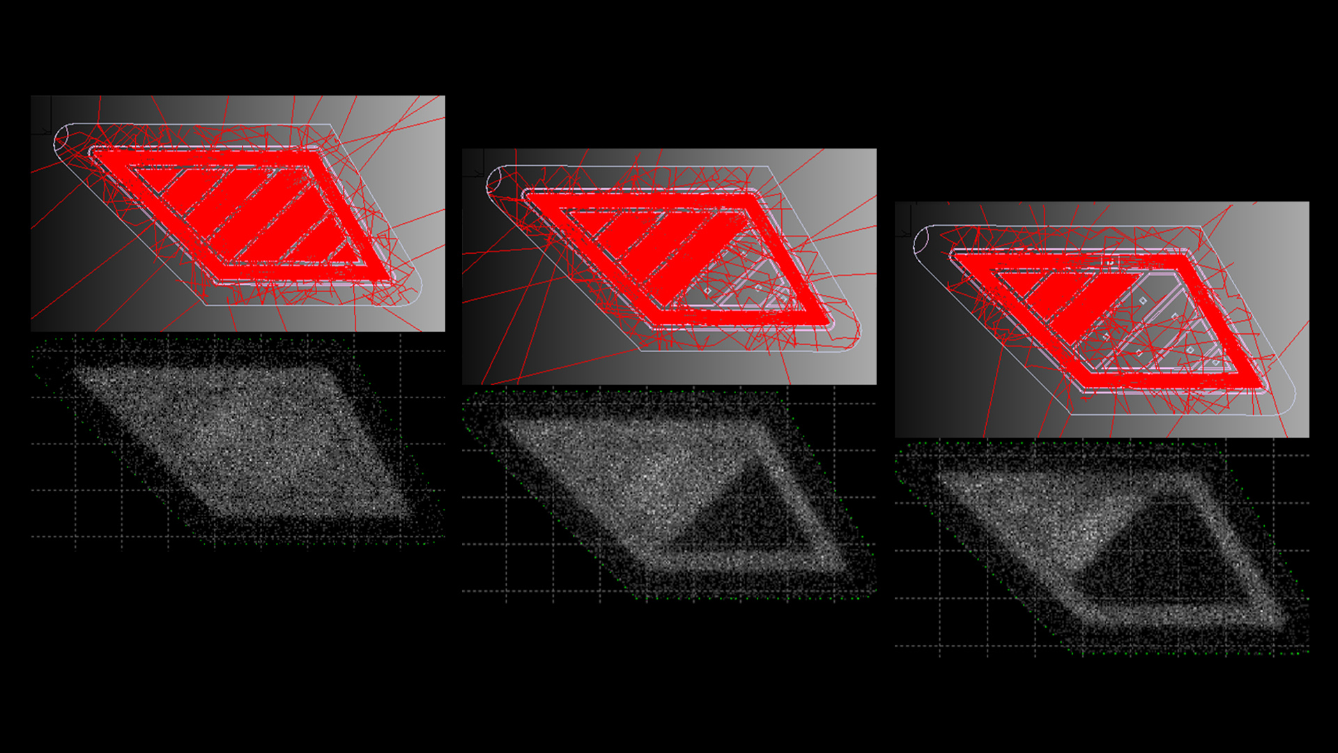
VCC offers a full suite of custom light pipe design and testing services. Using the latest light modeling software, our team can run light simulations, such as ray tracing, to track the path of light through the light pipe to devise the right solution. The design is then revised and optimized until the ideal optical requirements are met.
Step 3: Light Pipe Prototype
VCC helps you cut development times using rapid prototyping techniques for plastic components. We use a 3D printer to prototype the light pipe and further test it prior to tooling the custom solution, ensuring the optimal viewing angle and lighting properties are achieved.
Step 4: Tooling & Production
When the light pipe prototype is approved, it’s time to move into tooling. Because the 3D prototype we provide is 90% accurate to the finished product, you can feel confident investing in the tooling after you’ve validated the design. Once tooling is complete, we fabricate and assemble our components in our state-of-the-art facility in Mexico, ensuring you receive the utmost level of quality, plus the many advantages nearshore manufacturing provides.
The whole process can take as little as 2 weeks or as long as 12 — it all depends on the complexity of the design.
Over the last few years, 3D printing has changed the game in light pipe prototyping, allowing some manufacturers to use in-house printers to dramatically reduce production times. Shaving days or weeks off of a timeline is a huge benefit for designers and OEMs, but 3D printing can also provide a less common advantage: completing small light pipe runs to be used in actual products.
VCC’s in-house 3D printer can print light pipes using photopolymer resin with different additives then hand polish them for use in products. These in-house printed pipes can match approximately 82-95% of the light characteristics delivered by going the injection molding route. In this case, doing a small pilot run could give OEMs and designers the quantity they need to verify the concept of their final product.
In this case, doing a small pilot run could give OEMs and designers the quantity they need to verify the concept of their final product.
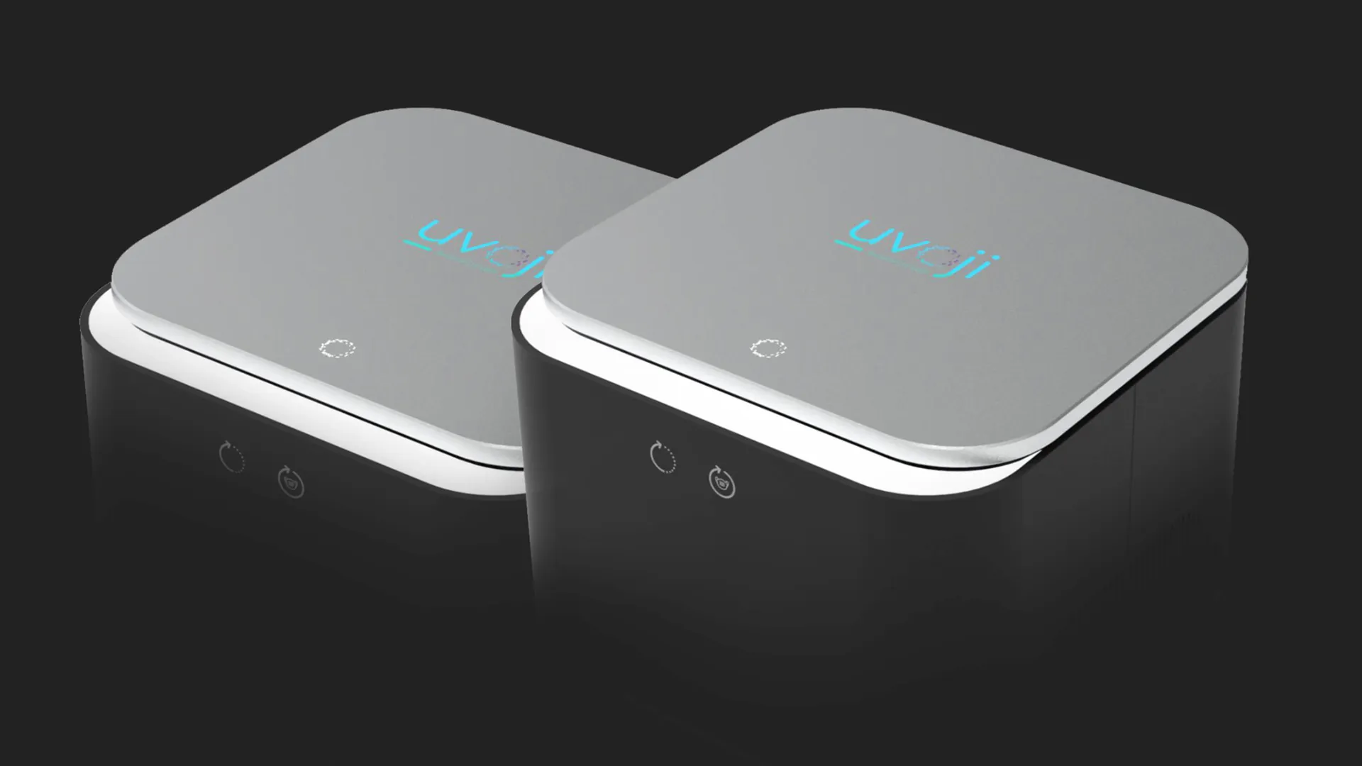
For example, even complex custom light pipe concepts like this non-surgical medical device can be validated quickly and efficiently with our in-house 3D printing capabilities.
A well-designed human-machine interface (HMI) can deliver faster throughput and reduced downtime. Custom, flexible — and even rigid — light pipes open up a wide range of design possibilities by providing greater flexibility and control.
Making indicator decisions early on in the design process can help you maximize efficiencies and get exactly what you want in the finished design. This includes visibility of status indicators from distances that help the end user maintain safe and reliable operation.
To learn more, check out the VCC’s custom light pipe solutions or explore our robust light pipe portfolio.
Not all PCB assembly partners are the same. To ensure your boards stack up, choose a PCB assembly company that provides:
- PCB assembly, all in one place - one central point of contact for everything from concept and design to final assembly, including:
Preliminary design and layout
Prototype development
Manufacturing integration
Production - North American manufacturing - facilities close to home can cut down on product lead times, as well as shipping and production costs.
- In-house capabilities - if your PCB manufacturer is sending your work out, you are likely paying more in time and production costs. Find a one-stop shop with the core capabilities to handle every aspect of your PCB assembly, including surface mount technology and 3D printing for expedited prototyping and production.
- Stringent quality control processes - don’t take a chance on quality. See proof and documentation of testing and regulatory compliance, including ROHS.
- Proven PCB experience - make sure your PCBA partner has an outstanding on-time delivery so you get your components when you need them, every time.
- UL certification - last but not least, look for your PCB supplier’s UL Certification to ensure your PCB has been tested to meet fire safety standards using the UL94 flammability rating and UL796 standard for PCBs specifically.
- RoHS compliance - product-level adherence to the European Union’s Directive of the use of certain hazardous substances in electrical and electronic equipment (“RoHS”) may also be required. Our team provides documentation of RoHS compliance, as well as any other regulatory requirements.
UL Certification and the UL mark are invaluable for manufacturers and consumers. Certification is earned only after a series of stringent safety and performance tests.
For customers:
- Identifying which manufacturers’ processes and products meet UL’s strict standards is as simple as looking for the mark.
- Only UL-certified suppliers can provide components for a UL-listed finished product, ensuring all key parts are made with the same quality and safety requirements.
- If maintenance or repair is ever needed, the UL certification helps source the appropriate parts for safe, reliable performance.
For manufacturers:
- UL certification is the perfect way to substantiate claims of quality, safety, and performance.
- Obtaining a UL certification allows the manufacturer’s PCBA products to be sold worldwide.
- Rigorous third-party testing helps improve processes and products.
VCC is UL Rated for PCBA manufacturing, and our certificate number is E520330. All of our PCBA components use substrates and other materials that meet UL requirements.
Whether you need PCB assemblies with surface-mount or through-hole technology, VCC can customize your components with comprehensive PCBA design and production capabilities — right here in North America. With nearly 25,000 square feet of production space and 3 SMT lines, we offer full production and can scale to accommodate runs of any size.
Explore our extensive in-house PCB assembly capabilities, or contact our team.


