
In the complex world of modern electronics manufacturing, the journey from concept to product is full of challenges. At the heart of this journey is Printed Circuit Board Assembly (PCBA), the critical pcb assembly process that turns a bare circuit board into the heart of any electronic device. For Original Equipment Manufacturers (OEMs), pcb designers and product designers, making sure a PCBA is not only functional but also efficient, cost effective and reliable to produce is key. That’s where Design for Manufacturability (DFM) comes in to optimize the whole process in the electronics manufacturing industry.
At VCC, we don’t see DFM as a checklist; it’s a proactive engineering philosophy deeply embedded in our PCBA services. We challenge every stage of the design process – from system level architecture to component placement – to ensure manufacturability, cost effectiveness and product quality.
Why Design for Manufacturability (DFM)
DFM is a systematic approach to integrate manufacturing into the initial design phase of a Printed Circuit Board. It encompasses Design for Fabrication (DFF) and Design for Assembly (DFA) to prevent, detect, quantify, and reduce inefficiencies and waste throughout the whole PCB manufacturing lifecycle. The benefits of a robust DFM strategy are:
● Cost Savings: By identifying and mitigating potential manufacturing issues early, DFM reduces rework, scrap, and costly redesigns. It optimizes material usage and leverages economies of scale.
● Faster Time-to-Market: DFM streamlines the whole production process, resulting in fewer design iterations and quicker transition from concept to mass production. This accelerates product development and delivery, giving you a competitive edge.
● Better Products: Following DFM principles ensures PCBs are designed to meet all specifications and standards, overcoming limitations that can compromise quality. This results in better, more reliable products with higher performance and durability.
● More Flexibility and Scalability: DFM enables manufacturers to adapt to varying production volumes, scaling up or down as needed to meet market demand.
● Supply Chain Resilience: DFM processes can include alternative component choices to mitigate component shortages and lead time issues, to strengthen supply chain stability.
VCC’s DFM Process: A Phased Approach to PCBA
VCC’s PCBA services are built around a structured DFM process, integrated into three stages of the PCB design process. This systematic approach ensures that every aspect of the board is optimized for manufacturability and cost-effectiveness.
1. Design Phase: This initial and most critical phase focuses on the overall PCB layout. Our engineers work closely with OEMs to define the correct footprint and component packaging, so the design is aligned with manufacturing capabilities from the start. We verify the PCB design against manufacturing rules and capabilities, often using integrated DFM rules from advanced design tools. This proactive approach ensures first-pass manufacturing success by identifying and preventing costly errors and rework before they happen. During this phase, critical electrical and mechanical parameters are set and managed, laying the foundation for a reliable and manufacturable PCB.
2. Component Placement Phase: Following the foundation design, this stage focuses on precisely placing components on the board. We follow predefined placement rules to ensure adequate spacing between elements, thereby preventing assembly issues such as solder bridging or insufficient solder coverage. This attention to spacing also ensures that all necessary solder masks are applied correctly for proper soldering and component mounting, which impacts automated assembly processes and board density.
3. Routing Phase: The final phase involves routing the conductive paths (traces) on the PCB. This requires wiring standards and signal integrity requirements, especially critical for high-speed designs. We set precise spacing constraints for copper features, especially around back drills, to prevent electrical shorts and enhance PCB reliability. This phase also addresses protection from contamination and damage to ensure long-term performance and durability of the PCBA.
By following these three DFM process phases, VCC accelerates production, minimizes material waste, increases productivity, and reduces production time and cost to produce high-volume products.
DFM Rules for PCBA
Beyond the phased approach, VCC follows a set of DFM rules to guide every aspect of PCB design for manufacturability and performance:
● Maintain Design Clearance: We ensure adequate spacing between traces, pads, and components, following the manufacturer’s minimum clearance specifications to prevent short circuits and fabrication issues.
● Optimize Trace Widths: Trace widths are designed to handle the expected current without overheating. Wider traces for power circuits and signal traces optimized for signal integrity according to manufacturer guidelines.
● Minimize Layer Count: VCC can design and manufacture rigid and flexible PCBs up to 4 layers thick, but we strive to use the minimum number of layers while maintaining design integrity. This reduces manufacturing cost and complexity.
● Use Standard Via Sizes: We utilize common via sizes to simplify production, reduce manufacturing time, and lower costs. For high-density designs, VCC utilizes microvias—tiny, laser-drilled holes that connect selected layers, enabling higher component density and improved signal performance without compromising reliability. These microvias are significantly smaller than traditional through holes, enabling narrower trace widths and more compact routing.
● Place Fiducial Markers: Fiducial markers are placed on the PCB to aid automated optical inspection (AOI) and pick-and-place machine alignment, ensuring accurate component placement during assembly.
● Avoid Component Overlaps: Components are spaced to prevent soldering defects during automated assembly. Insufficient spacing can cause solder bridging or opens.
● Follow Aspect Ratio Guidelines: The aspect ratio (board thickness to drill diameter) is typically maintained at a ratio of 10:1 or less to ensure robust hole plating and long-term reliability.
● Define Controlled Impedance Properly: For high-speed designs, VCC specifies and manages controlled impedance requirements. This involves the precise management of electrical characteristics within traces and transmission lines to ensure that signals propagate without distortion or loss, thereby minimizing electromagnetic interference (EMI) and crosstalk.
● Label Key Information Clearly: Essential labels for part numbers, polarity markings, and test points are included to aid in testing, assembly, and troubleshooting, reducing human error.
● Account for Tolerances: Designs are developed with fabrication tolerances in mind, avoiding tight specifications that could increase cost and potential delays.
The VCC DFM Advantage: Integrated Expertise and Technology
VCC’s ability to deliver PCBA solutions is built on our integrated approach, combining multidisciplinary engineering expertise with state-of-the-art manufacturing capabilities:
● Multidisciplinary Engineering Team: Our in-house team of mechanical, optical, and electrical engineers works closely with OEMs from the initial engineering drawing phase to ensure design goals and optical requirements are met with precision.
● Simulation and Prototyping: VCC utilizes the latest light modeling software and ray tracing technology to perform light simulations, virtually eliminating light losses and optimizing designs for optimal optical requirements. Rapid prototyping with 3D printing provides 90% accurate prototypes, reducing tooling investment and development time.
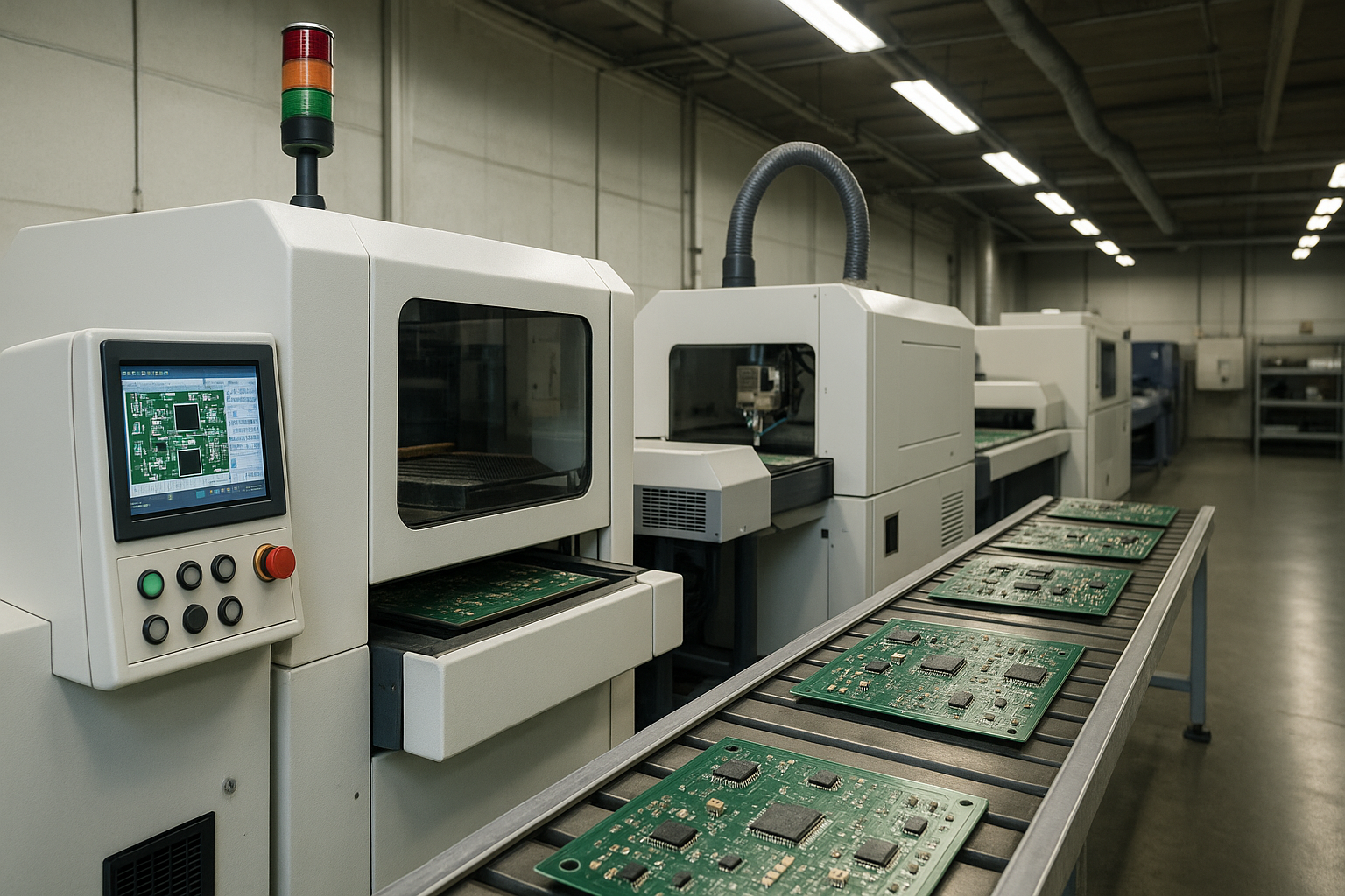
● Automated Assembly Capacity: Our state-of-the-art manufacturing facility features an automated mounting capacity of up to 29,000 components per hour, enabling high-speed, high-volume, and consistent PCBA production.
● Quality Control: Every PCBA undergoes comprehensive quality and functional testing, including visual inspection, Automated Optical Inspection (AOI), and X-ray inspection, to detect any non-conformance issues, such as soldering defects or component misalignment. VCC is ISO 9001 certified and adheres to IPC/WHMA-A-620 standards for cable and wire harness assemblies, ensuring the highest quality and reliability.
● Nearshore Manufacturing Advantage: With facilities in Carlsbad, CA, and Tijuana, Mexico, VCC offers nearshore manufacturing benefits: better quality control, predictable pricing, and a supply chain less affected by global tariffs.
Partner with VCC for DFM
In today’s competitive electronics market, designing for manufacturability is not an option—it’s a must. VCC’s DFM expertise, combined with our capabilities and quality commitment makes us the right partner for your next PCBA project. We don’t just build components, we engineer solutions that simplify your production, reduce cost and accelerate your time to market.


